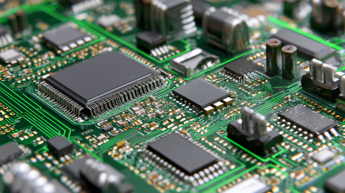
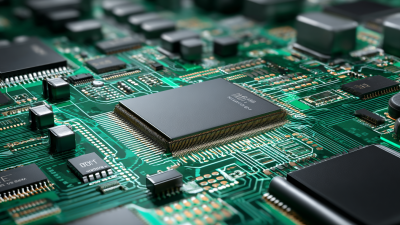
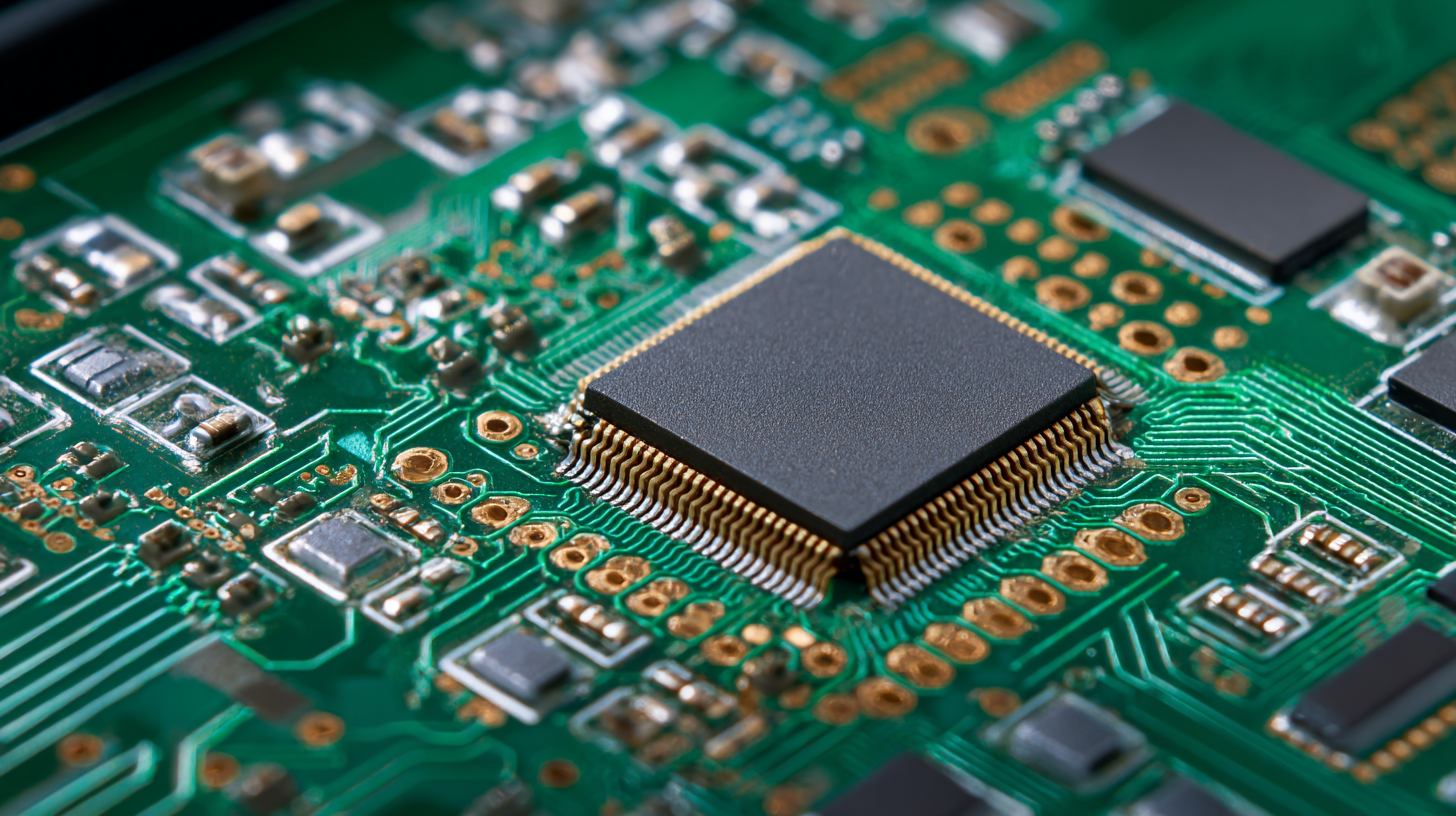
How to Optimize Your PCB Fabrication Process for Enhanced Efficiency and Quality
In the rapidly evolving landscape of electronics manufacturing, optimizing the PCB fabrication process is crucial for ensuring enhanced efficiency and quality. As printed circuit boards (PCBs) serve as the backbone of modern electronic devices, the need for meticulous design and production becomes increasingly significant. This article explores various strategies that can be employed to streamline the PCB fabrication process, addressing common challenges and highlighting best practices. From improving the design phase through advanced software tools to selecting the right materials and manufacturing techniques, each step in the PCB fabrication journey holds potential for optimization. By implementing these optimizations, manufacturers can not only reduce lead times and costs but also elevate the overall quality of the final product, thereby meeting the stringent demands of today's competitive market.
Understanding Key Metrics for PCB Fabrication Efficiency Improvement
To enhance efficiency and quality in PCB fabrication, understanding key metrics is essential. One crucial metric is Yield Rate, which measures the percentage of functional boards produced relative to the total number fabricated. According to IPC's 2022 study, achieving a Yield Rate of 98% or higher can significantly reduce costs associated with rework and minimize waste, thus enhancing overall efficiency. Monitoring this metric helps manufacturers identify issues in the production line early, allowing for timely interventions.
Another critical metric is Turnaround Time (TAT), which tracks the duration from order placement to final delivery. A report by Research and Markets highlighted that PCB manufacturers optimizing their TAT can improve customer satisfaction rates by up to 30%. By adopting strategies like lean manufacturing and just-in-time production, companies can streamline their processes and reduce TAT, leading to faster delivery times. Additionally, Capacity Utilization Rate is an important measure that reflects how effectively a facility's production capacity is being used; higher utilization rates indicate better efficiency and resource management, crucial for maintaining quality in the competitive PCB market.
Implementing Design for Manufacturability (DFM) Principles in PCB Design
Implementing Design for Manufacturability (DFM) principles is crucial for optimizing the PCB fabrication process, ensuring both enhanced efficiency and superior product quality. DFM focuses on simplifying the design and manufacturing stages, thereby reducing production defects and costs. According to a recent industry report by IPC, implementing DFM practices can lead to a 30% reduction in manufacturing costs and a significant decrease in product cycle time. By considering manufacturing constraints during the design phase, engineers can create PCBs that are easier to produce, which in turn results in faster time-to-market and improved reliability.
Tips for implementing DFM principles include focusing on component placement and spacing. Properly arranged components can facilitate efficient soldering and reduce the likelihood of errors during assembly. Additionally, using standard component sizes can minimize setup times and costs. Another vital aspect is the design of the PCB layout, where ensuring adequate routing and avoiding complex geometries will enhance manufacturability. A report from the IEEE highlights that 70% of PCB failures are attributed to design-related issues, underscoring the importance of carefully considering DFM during the design process to mitigate risks and enhance yield.
How to Optimize Your PCB Fabrication Process for Enhanced Efficiency and Quality
| Parameter |
Current Value |
Target Value |
DFM Impact |
| Assembly Yield (%) |
85 |
95 |
Increase in design clarity and reduced errors |
| Production Lead Time (days) |
20 |
10 |
Streamlined designs lead to faster assembly |
| Cost per PCB ($) |
5.00 |
4.00 |
Optimized component placement reduces cost |
| Failure Rate (%) |
5 |
1 |
Adoption of DFM practices lowers defects |
| Stakeholder Satisfaction (%) |
70 |
90 |
Improved quality enhances customer confidence |
Utilizing Advanced Materials and Technologies to Enhance PCB Quality
Utilizing advanced materials and technologies is crucial in optimizing the PCB fabrication process, leading to enhanced efficiency and quality. One key aspect is the incorporation of
high-performance substrates, such as polyimide or ceramic-based materials, which provide superior thermal stability and electrical insulation.
These materials not only improve the thermal management of PCBs but also enable the design of more complex circuit architectures. The use of such advanced materials helps reduce potential failures and extends the lifespan of electronic devices.
In addition to materials, implementing cutting-edge technologies like automated soldering and imaging systems can significantly streamline the fabrication process. Automation reduces human error and increases precision, ensuring that each component is placed accurately on the PCB.
Moreover, adopting technologies like 3D printing for prototyping can accelerate the development phase, allowing for rapid iterations and testing without compromising quality.
By leveraging these advancements, manufacturers can achieve a higher standard of PCB quality while also optimizing production workflows, ultimately meeting the increasing demands of modern electronic applications.
Streamlining Supply Chain Management for Timely PCB Production
Effective supply chain management is crucial for timely PCB production, as it directly influences lead time variability, inventory levels, and production scheduling. By understanding the impact of lead time fluctuations, companies can identify the potential bottlenecks in their production lines. This insight allows for the implementation of strategies aimed at minimizing delays, ultimately ensuring that products meet market demand without compromising quality.
Moreover, adopting just-in-time inventory practices can enhance responsiveness in the supply chain. By aligning inventory levels more closely with production needs, businesses can reduce excess stock and associated costs while maintaining sufficient materials for PCB fabrication. Regular communication with suppliers and adopting agile practices can further streamline operations, ensuring that lead time variability does not disrupt the overall production timeline. These steps not only promote efficiency but also contribute to higher quality PCB products, as timely access to materials allows for a more controlled and consistent manufacturing process.
Adopting Automated Testing Procedures to Reduce PCB Defects and Rework
 Adopting automated testing procedures is crucial for enhancing the efficiency and quality of the PCB fabrication process. By integrating automated testing into your workflow, you significantly reduce the likelihood of errors that can lead to defects. Automated systems provide real-time monitoring and analysis, allowing you to identify issues as they arise rather than after the fact. This proactive approach not only minimizes rework but also accelerates the production timeline, leading to overall improved throughput.
Tip: Implement boundary scan testing early in your process. This technique allows you to test interconnections on PCBs without needing physical access to pins, which helps in rapidly identifying fault locations.
Moreover, automated testing can standardize procedures across your production floor, ensuring that every board meets the same rigorous quality standards. By utilizing software that automates the testing process, you can ensure consistency and reliability, reducing human error effectively.
Tip: Integrate a feedback loop within your automated system that updates your fabrication processes based on test results, ensuring continuous improvement and quicker adaptations to any design changes.