How to Optimize PCB Design and Assembly for 2026?
As we approach 2026, optimizing PCB design and assembly becomes critical for tech industries. A report by IPC stated that the global PCB market is projected to reach $85 billion by 2026, highlighting the escalating demand. Efficiency in PCB design and assembly can drive cost reductions and enhance product performance.
Industry expert Dr. Lisa Wang emphasizes the need for innovation in this field: "The future of PCB design and assembly lies in automation and sustainable practices." Companies that adapt to new technologies will excel. However, many still rely on outdated methods, risking obsolescence. Embracing advancements can be challenging yet necessary for success.
Market pressures for faster production cycles and reduced costs can cloud decision-making. Implementing best practices requires reflection on current strategies and a willingness to change. The path to optimization isn't straightforward, but understanding mistakes transforms setbacks into opportunities in PCB design and assembly.

Current Trends in PCB Design for 2026
The landscape of PCB design is evolving rapidly as we look toward 2026. One major trend is the rise of ultra-thin PCBs. These boards save space and weight, making them ideal for compact devices. However, thinner materials can lead to durability issues. Designers must balance design innovation with reliability. This challenge pushes engineers to explore new substrate materials.
Flexible PCBs are also gaining traction. These boards bend and twist, fitting into unusual spaces. They are perfect for wearables and IoT devices. Yet, the manufacturing process for flexible boards can be complex. Tighter tolerances may cause defects, which need careful monitoring. Testing phases must be rigorous to ensure quality.
Sustainability is another focal point. Designers are increasingly choosing eco-friendly materials. Recyclability and energy efficiency are priorities. This shift can be costly, and not all manufacturers are on board. Investing in green technologies requires foresight and commitment. However, the long-term benefits can outweigh short-term challenges. Embracing these trends will shape a new era in PCB design.
How to Optimize PCB Design and Assembly for 2026? - Current Trends in PCB Design for 2026
| Trend |
Description |
Impact on Design |
Year of Adoption |
| Flexible PCBs |
Increased demand for lightweight and compact electronics. |
Encourages innovative designs that save space. |
2026 |
| Advanced Simulation Tools |
Use of AI-enhanced software for design validation. |
Reduces errors and improves efficiency in the design process. |
2025 |
| Sustainable Materials |
Adoption of eco-friendly materials for PCB manufacturing. |
Promotes environmentally responsible products. |
2026 |
| 3D Printing |
Integration of 3D printing in PCB prototyping and production. |
Faster turnaround times and customization possibilities. |
2025 |
| Miniaturization |
Increasing the density of components on PCBs. |
Challenges engineers to optimize layouts and thermal management. |
2026 |
Key Factors Influencing PCB Assembly Efficiency
Optimizing PCB design and assembly is crucial for efficiency. Several key factors influence this process. Design accuracy is vital. Errors in layout can lead to costly rework. Ensure that components are correctly placed and routed. Small mistakes can have big consequences.
Tips: Always double-check design files. Use simulation tools to predict performance. This reduces the chance of errors.
Component selection plays a significant role. Choosing the right materials is essential for durability. Consider the operating environment and the end-use of the PCB. If the board is used in high-temperature settings, choose materials that can withstand heat.
Tips: Look for materials with high thermal conductivity. This can enhance performance. Keep an eye on lead times, as some components may take longer to source.
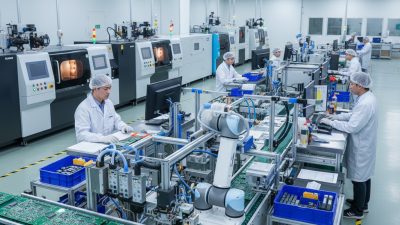
Assembly techniques also impact efficiency. Incorporate advanced technologies, like pick-and-place machines. Ensure that workers are well-trained in these methods. A skilled team can spot inefficiencies quickly. It's crucial to refine processes continually.
Tips: Conduct regular training sessions. Share insights from past assembly jobs. Learning from mistakes can lead to better outcomes in future projects.
Best Practices for Sustainable PCB Manufacturing
Sustainable PCB manufacturing is crucial as we approach 2026. A growing number of companies are focusing on eco-friendly materials and processes. According to industry reports, nearly 70% of PCB manufacturers seek to adopt greener practices. This shift is partly due to increased consumer demand for sustainable electronic products.
Using lead-free solder and recyclable substrates can significantly reduce the environmental impact. Studies show that employing bio-based materials can lessen harmful emissions by up to 40%. However, challenges remain. Many manufacturers still rely on traditional methods that are not environmentally friendly. Transitioning to sustainable practices requires investment and training.
Waste management is another area needing improvement. Often, leftover materials are discarded, creating unnecessary waste. Developing efficient recycling processes should be a priority. Reports indicate that ineffective waste handling can cost companies up to 20% of their operational budget. Addressing these issues will be vital for sustainable growth in PCB design and assembly.
Emerging Technologies in PCB Design and Assembly
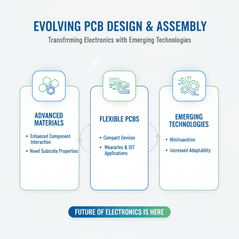
The landscape of PCB design and assembly is rapidly evolving. Emerging technologies are at the forefront of this transformation. Advanced materials, for example, are altering how components interact. Flexible PCBs are becoming popular for compact devices. Their adaptability allows for new applications in wearables and IoT devices.
Automation is another vital technology. It streamlines assembly processes, improving efficiency. However, over-reliance on automation can create challenges. Human oversight remains essential to ensure quality. Improper calibration can lead to defects, impacting the final product. Regular assessments are crucial to mitigate these risks.
Another trend is the shift toward sustainable practices. Eco-friendly materials are gaining traction in PCB production. Yet, the transition needs careful management. Not every solution suits every product. It requires exploration and sometimes disappointing failures to find the best fit. Addressing these emerging technologies demands a balanced approach, embracing both innovation and reflection.
Future Challenges in PCB Development and Solutions
The PCB industry faces several future challenges as we approach 2026. One major issue is the increasing complexity of electronic devices. According to a recent industry report, the demand for multilayer PCBs has risen by 25% over the past few years. As more components get packed into smaller devices, design and assembly become significantly more challenging. Optimizing layouts and minimizing signal interference is crucial.
Tip: Make use of advanced simulation tools. They can help visualize potential issues before physical production. Simulating thermal and electrical performance is vital for success.
Another challenge is sustainability. More consumers are concerned about electronics waste. In 2022, an estimated 58 million tons of e-waste were generated globally. PCB manufacturers must adopt eco-friendly materials and recycling practices. This shift requires innovative approaches to production and materials selection. It’s not just about compliance but also about meeting customer expectations.
Tip: Consider using biodegradable materials where possible. They can reduce environmental impact and resonate with eco-conscious customers.
Despite these challenges, the focus on technology advancement provides opportunities. Engineers must adapt quickly to evolving trends. Stagnation can lead to obsolescence. The road to optimizing PCB design and assembly will demand continuous learning and adaptation. Staying informed about regulatory changes is essential too.