2025 How to Master PCB Design and Assembly for Beginners and Experts
In the rapidly evolving world of electronics, mastering PCB design and assembly has become an essential skill for both beginners and seasoned professionals alike. With the proliferation of smart devices and the Internet of Things (IoT), the demand for efficient and effective PCB design and assembly techniques is at an all-time high. This article aims to provide a comprehensive guide for those looking to navigate the complexities of PCB design and assembly, ensuring that readers develop a strong foundation in the principles and practices necessary for success in this field.
Whether you are just starting your journey or seeking to refine your existing skills, understanding the intricacies of PCB design and assembly is crucial. From the basic components and layout considerations to advanced techniques that enhance performance and manufacturability, this guide will cover essential topics. As we delve into the nuances of PCB design and assembly, we will explore the tools, methodologies, and best practices that can elevate your projects, ensuring that both beginners and experts are equipped to tackle the challenges posed in today's competitive landscape.

Understanding the Fundamentals of PCB Design: Principles and Techniques
Understanding the fundamentals of PCB design requires a grasp of essential principles and techniques that cater to both beginners and experts in the field. The foundation of PCB design starts with understanding the role of each component in the circuit. With the global printed circuit board market expected to reach approximately $88 billion by 2025, as indicated by a recent industry report, mastering these fundamentals becomes increasingly important for professionals seeking to innovate and optimize electronic designs. Key principles involve a strong grasp of electrical theory, including Ohm's Law and Kirchhoff's laws, which guide the designer in creating effective and efficient circuit layouts.
In addition to theoretical knowledge, practical techniques such as schematic capture and layout design are crucial. Utilizing software tools for PCB design enables designers to visualize and manipulate the circuits effectively. Recent studies show that improper layout techniques can result in a reduction of performance by up to 30%, highlighting the need for adherence to best practices in trace routing, component placement, and impedance control. Techniques such as maintaining appropriate clearances and understanding thermal management are essential to prevent issues such as signal integrity loss and overheating, which can jeopardize the reliability of electronic devices.
By mastering these critical principles and techniques, individuals can ensure their designs meet the increasing demands of modern electronics.
Key Software Tools for PCB Design: A Comparative Analysis for Beginners
When venturing into the world of PCB design, selecting the right software tools is crucial for both beginners and experts. Many software solutions offer unique features that cater to different aspects of the design process, from schematic capture to layout and simulation. For beginners, ease of use and a friendly interface are vital as they navigate through the complexities of PCB design. Tools that provide intuitive workflows, drag-and-drop functionalities, and extensive tutorials can significantly ease the learning curve, allowing new users to grasp foundational concepts quickly.
On the other hand, more experienced designers may seek advanced features such as multi-layer handling, comprehensive simulation capabilities, and robust collaboration functionalities. These experts often prioritize software that integrates seamlessly with other engineering tools and supports complex designs with precision. A comparative analysis of various software tools can help identify the best fit based on project requirements, budget, and the specific skill level of the user. By understanding the distinctive offerings and limitations of each tool, PCB designers can optimize their workflow, improve design accuracy, and enhance overall productivity.
2025 How to Master PCB Design and Assembly for Beginners and Experts - Key Software Tools for PCB Design: A Comparative Analysis for Beginners
| Software Tool |
Ease of Use |
Price Range |
Key Features |
Target User |
| Eagle |
Beginner-Friendly |
Free - $100/month |
Schematic Capture, Board Layout, Libraries |
Hobbyists, Students |
| KiCad |
Moderate |
Free |
Open-Source, 3D Viewer, Extensive Documentation |
All Levels |
| Altium Designer |
Advanced |
$1000+/year |
High-End Features, Unified Environment, Libraries |
Professionals |
| EasyEDA |
Very Easy |
Free - $10/month |
Online Platform, Community Support, Schematic & PCB |
Beginners |
| OrCAD |
Moderate to High |
$500+/year |
Extensive Analysis Tools, Integration with MATLAB |
Engineers, Advanced Users |
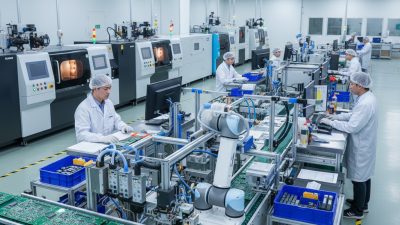
Best Practices in PCB Assembly: Ensuring Quality and Reliability
When it comes to PCB assembly, ensuring quality and reliability is paramount. Quality control should be integrated into every step of the assembly process, from design validation to final inspection. Implementing stringent checks at various stages helps to catch potential issues before they escalate. Regularly updating your design rules based on the latest industry standards can significantly reduce the likelihood of defects and enhance the overall reliability of the finished product.
Tips: One effective tip for maintaining quality is to conduct a Design for Manufacturability (DFM) review early in the design process. This ensures that the design is not only feasible but also optimized for assembly, minimizing errors that could arise during production. Additionally, incorporate automated optical inspection (AOI) systems in your assembly line to detect defects in real-time, facilitating prompt corrections.
Another crucial aspect is the selection of appropriate materials and components. Reliable sourcing of high-quality parts should never be overlooked, as subpar components can lead to failures in functionality. Establishing strong relationships with reputable suppliers can provide access to reliable parts that meet stringent quality standards.
Tips: Always maintain an up-to-date list of preferred suppliers and alternates, which can help in situations where specific components are unavailable. Additionally, consider the use of advanced soldering techniques to enhance joint reliability, especially in high-stress applications.
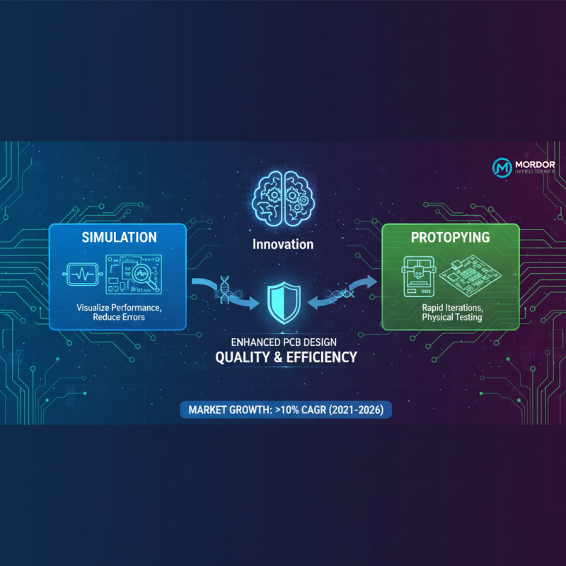
Advanced Techniques in PCB Design: Integrating Simulation and Prototyping
The integration of simulation and prototyping in PCB design is pivotal for both beginners and experts aiming to enhance their skills. As the industry increasingly demands high-quality and efficient electronic products, the incorporation of advanced simulation techniques has become essential. According to a report by Mordor Intelligence, the PCB design software market is projected to grow at a CAGR of over 10% from 2021 to 2026, highlighting the growing reliance on these technologies. Simulation tools enable designers to visualize how a circuit will perform under various conditions, reducing the risk of errors and facilitating faster design iterations.
Prototyping, often the next step after initial simulations, bridges the gap between design and functionality. Engaging in rapid prototyping allows designers to create physical models of their circuits, which is invaluable for practical testing and validation. A study by the IPC (Institute for Interconnecting and Packaging Electronic Circuits) found that utilizing prototypes can decrease time-to-market by approximately 50% in many projects. This time-saving advantage not only ensures that products are launched faster but also enhances collaboration between teams, fostering innovation through iterative testing and improvement. As PCB technology evolves, mastering these advanced techniques of simulation and prototyping will be key to staying competitive in the field.
Future Trends in PCB Technology: Sustainability and Miniaturization Insights
The world of printed circuit boards (PCBs) is undergoing a significant transformation, driven primarily by trends in sustainability and miniaturization. As technology advances, manufacturers are increasingly mindful of the environmental impact of PCB production. This shift is evident in the adoption of eco-friendly materials, such as biodegradable substrates and halogen-free laminates, which offer reduced toxicity and improved recyclability. By prioritizing sustainability, businesses are not only complying with regulatory demands but also appealing to a conscientious consumer base that values green practices.
In parallel, miniaturization remains a key trend in PCB technology, reflected in the continuous demand for smaller, more efficient electronics. This has prompted innovations in design methodologies and fabrication techniques, such as advanced layering, embedded components, and finer pitch connections. These developments allow for higher component densities and performance in compact forms, catering to the needs of modern devices such as wearables, IoT devices, and smartphones. As both sustainability and miniaturization converge, the future of PCB design and assembly is set to become not only more efficient but also more aligned with global efforts to reduce environmental footprints.
Future Trends in PCB Technology
This chart illustrates the investment trends in various upcoming PCB technologies for 2025. Sustainability and miniaturization are the primary focus areas, with a significant portion of investments directed towards smart electronics and flexible PCBs.