Innovative Techniques for Efficient PCB Board Design You Need to Know
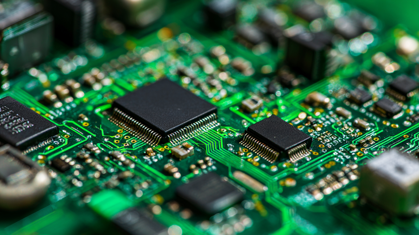
In the rapidly evolving world of technology, efficient PCB board design plays a crucial role in the development of innovative electronic devices. As advances in miniaturization and functionality continue, designers are challenged to meet higher performance standards while maintaining cost-effectiveness. Renowned PCB board design expert Dr. Emily Chang emphasizes the importance of innovation in this field, stating, "The future of electronics hinges on our ability to adapt and innovate in PCB board design."
With rising demands for compact and complex electronic systems, designers must leverage cutting-edge strategies and techniques that not only streamline the design process but also enhance product reliability and manufacturability. Recent trends indicate a shift towards integrating software tools, advanced materials, and automated processes that significantly improve the overall efficiency of PCB board design. By harnessing these innovative techniques, engineers can break through the limitations of traditional design methods and push the boundaries of what is possible in electronic circuit development.
In this comprehensive guide, we will explore some of the most effective and groundbreaking techniques for efficient PCB board design that you need to know. Whether you are a seasoned professional or just starting in the industry, understanding these methodologies is essential for staying ahead in the competitive landscape of electronics manufacturing.
Emerging Trends in PCB Design Efficiency: An Overview of Innovative Techniques
In recent years, the landscape of PCB design has been dramatically transformed by innovative techniques that enhance efficiency and reduce time-to-market. One significant trend is the integration of AI-driven design tools, which leverage machine learning to optimize layouts and reduce errors. According to industry reports, the adoption of AI in PCB design can lead to a 30% decrease in design time. Innovations like this are becoming essential as electronics manufacturers seek to stay competitive.
Moreover, the emergence of Lab-on-PCB technology exemplifies the shift towards multifunctional and compact designs. This approach not only streamlines the manufacturing process but also supports the growing demand for miniaturization in consumer electronics and medical devices. Recent advancements in bio-microsystem integration are set to reshape workflows, with projections indicating a market growth rate of 25% in the next five years. As these trends evolve, companies must embrace these technologies to enhance their product offerings and meet the dynamic needs of various sectors, including automotive and healthcare.
Impact of Simulation Software on PCB Design Time Reduction and Quality Assurance
The advent of simulation software has significantly transformed PCB design processes, enabling designers to reduce both design time and enhance quality assurance. The global PCB design software market size, valued at $3.17 billion in 2023, is expected to grow significantly, reaching $10.77 billion by 2032. This rapid growth is attributed to the increasing adoption of advanced simulation tools that facilitate real-time testing and validation of PCB layouts, ultimately optimizing the design workflow.
Moreover, the integration of AI technology within PCB fabrication presents opportunities for improved efficiency and quality control. AI-driven solutions provide data-driven insights that streamline design for manufacturability (DFM) processes, significantly reducing errors and production timelines. For instance, advanced simulation tools enable faster iterations and more reliable outputs, shortening time-to-market for new products. As designers increasingly leverage such innovative technologies, the combination of simulation software and AI not only accelerates the design phase but also assures high-quality outcomes, setting new industry standards for PCB development.
Advantages of High-Density Interconnect (HDI) Technology in PCB Manufacturing
High-Density Interconnect (HDI) technology has revolutionized PCB manufacturing by allowing for a more compact design while enhancing performance. According to the IPC's "Design and Manufacturing Guidelines for HDI PCBs," the use of HDI technology can decrease the size of PCBs by up to 50%, making it ideal for applications in compact and portable devices. The reduction in size is accompanied by a significant boost in interconnection capabilities, which can lead to a 30% increase in signal speed and reduced electromagnetic interference, resulting in more reliable electronics.
Employing HDI technology comes with clear advantages, especially in sectors that demand high performance and miniaturization, such as consumer electronics and telecommunications. As per a report by Market Research Future, the global HDI PCB market is expected to grow at a CAGR of 10% from 2021 to 2027, driven by the rise in demand for efficient, high-performance devices.
**Tip:** When designing PCBs utilizing HDI techniques, consider incorporating micro vias and blind/buried vias to optimize layer count and space.
**Tip:** Regularly update your design and manufacturing knowledge through industry webinars and trainings, as HDI techniques continuously evolve, keeping you abreast of the latest innovations.
Advantages of High-Density Interconnect (HDI) Technology in PCB Manufacturing
Sustainable Practices in PCB Design: Minimizing Waste and Energy Usage
Sustainable practices in PCB design are becoming increasingly crucial as the demand for electronic devices grows. One of the fundamental ways to minimize waste is through efficient material selection. Choosing materials that are recyclable or have a lower environmental impact can significantly reduce the ecological footprint of PCB production. Additionally, adopting design strategies that minimize the amount of material used—such as optimizing layout and integrating multiple functions into a single board—can further contribute to waste reduction.
Energy usage can also be addressed through innovative design techniques. Implementing power-efficient components and circuit topologies not only enhances the performance of the PCB but also reduces energy consumption during operation. Furthermore, utilizing advanced simulation tools during the design phase can help engineers predict performance issues and optimize energy efficiency before physical production begins. By prioritizing these sustainable practices, designers can create PCBs that are not only efficient and functional but also environmentally responsible.
Innovative Techniques for Efficient PCB Board Design You Need to Know - Sustainable Practices in PCB Design: Minimizing Waste and Energy Usage
| Technique |
Description |
Benefits |
Waste Reduction (%) |
Energy Savings (%) |
| Design for Manufacturing (DFM) |
Optimize designs to simplify manufacturing processes. |
Reduces manufacturing errors and costs. |
30% |
15% |
| Simulation Tools |
Use software to simulate PCB behavior before physical prototyping. |
Minimizes the number of prototypes needed. |
25% |
20% |
| Layer Reduction |
Design PCBs with fewer layers while maintaining performance. |
Lowers the material costs and energy during production. |
40% |
10% |
| Component Selection |
Choose eco-friendly and energy-efficient components. |
Reduced environmental impact and operational costs. |
35% |
25% |
| Design Rules Check (DRC) |
Automated checks to ensure designs meet manufacturing standards. |
Increases reliability and reduces rework. |
20% |
5% |
Harnessing AI and Machine Learning for Enhanced PCB Design Decisions and Output
The integration of AI and machine learning has revolutionized the field of PCB design, enabling engineers to make informed decisions that enhance productivity and efficiency. These technologies analyze vast datasets, identifying patterns and generating insights that can lead to optimized layouts and reduced manufacturing errors. By simulating various design scenarios, AI algorithms can predict potential issues early in the design phase, allowing for timely adjustments and a more streamlined development process.
Moreover, machine learning models can continuously improve over time. As they process more data from past designs, they refine their recommendations, promoting best practices and innovative solutions tailored to specific project requirements. This adaptability not only helps designers to keep pace with the growing complexity of electronic systems but also fosters a culture of innovation within engineering teams. Harnessing AI-driven tools can ultimately result in cost savings and shorter time-to-market for new products, marking a significant leap forward in PCB design efficiency.