
How to Choose the Right Printed Circuit Board?
Choosing the right printed circuit board begins with understanding the product, not browsing a supplier catalog. A compact sensor may need a two-layer FR-4 board with controlled grounding. A high-speed controller may require more layers, precise impedance, and careful signal routing. I have seen promising designs struggle because heat, vibration, or connector stress was considered too late. Small choices matter.
Material selection should match the operating environment. Standard FR-4 suits many indoor electronics, while high-temperature or flexible materials may support demanding applications. Copper thickness, board layers, surface finish, and component density also affect cost and reliability. A thicker copper layer can carry more current, but it may complicate manufacturing. Nothing is free. Designers should confirm voltage, current, frequency, temperature, moisture, and mechanical limits before placing an order. These details create a practical specification for comparing manufacturers and quotations.
Reliable suppliers provide design-for-manufacturing feedback, material certifications, inspection records, and electrical testing. They should explain tolerances clearly rather than promise unrealistic results. Independent standards, such as IPC guidance, can support consistent quality decisions, although compliance alone does not guarantee a perfect product. I still recommend reviewing prototypes under real conditions. A board that passes a basic bench test may behave differently inside a sealed enclosure. That lesson is easy to overlook. The best choice balances performance, production volume, lifecycle cost, and repair needs. It also leaves room for honest revision when early assumptions prove wrong.
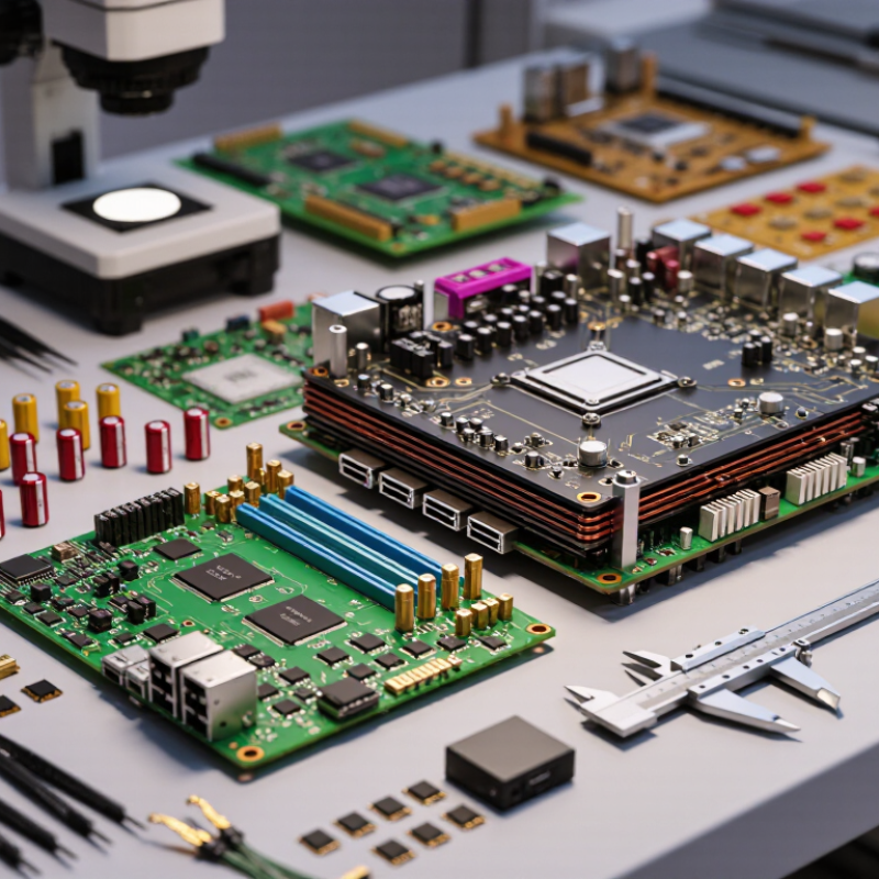
Define Electrical and Mechanical Requirements Under IPC-2221
How to Choose the Right Printed Circuit Board?
Under IPC-2221, PCB selection begins with measurable electrical and mechanical requirements. Record operating voltage, maximum current, signal frequency, temperature, and expected service life. These values control insulation spacing, copper thickness, trace width, and impedance. IPC-2221B explains that clearance depends on voltage, environment, coating, and altitude. A fixed spacing rule is risky. It may pass a bench test and fail in humid equipment.
Mechanical details matter just as much. Define board length, width, thickness, mounting-hole positions, connector forces, bend zones, and enclosure limits. Specify the layer stackup before routing. For high-speed signals, request controlled impedance and confirm the dielectric thickness with the fabricator. Thermal expansion also deserves attention. IPC-2221 addresses coefficient of thermal expansion and temperature limits, while IPC-6012 adds qualification expectations for rigid boards. Small holes. Large consequences.
Industry data supports this discipline. IPC’s 2024 Electronics Industry Sentiment Report identified material costs, supply stability, and delivery performance as continuing industry concerns. These pressures make early requirement control practical, not ceremonial. In my own design reviews, the missed detail is often mechanical: a hole shifts by one millimeter, or a connector collides with the housing. Recheck the drawing. I still find assumptions after approval. That is the uncomfortable part. A complete requirement sheet should include test conditions, tolerances, inspection methods, and acceptance criteria, with sources such as IPC-2221B and IPC-6012 clearly referenced.
How to Choose the Right Printed Circuit Board? - Define Electrical and Mechanical Requirements Under IPC-2221
| Requirement Area | Key Design Parameter | Typical Selection or Starting Point | Why It Matters Under IPC-2221 | Design Verification |
|---|---|---|---|---|
| Electrical | Nominal operating voltage | Define normal, peak, transient, and mains-related voltage levels before setting conductor spacing. | Conductor spacing must control the risk of electrical breakdown and surface flashover. | Check external and internal spacing against the applicable voltage, environment, insulation system, and end-use safety requirements. |
| Electrical | Creepage and clearance | Use larger spacing for higher voltage, pollution, moisture, contamination, or reduced insulation reliability. | Clearance is measured through air; creepage follows the insulating surface. Both affect insulation performance. | Measure the shortest applicable paths in the layout and review slots, cutouts, vias, pads, and component bodies. |
| Electrical | Current capacity | Size trace width and copper thickness from current, allowable temperature rise, conductor length, and thermal conditions. | A trace that is electrically continuous may still overheat or create excessive voltage drop. | Calculate resistance, voltage drop, power dissipation, and temperature rise for continuous and peak current. |
| Electrical | Signal integrity | Define impedance, rise time, edge rate, routing length, return path, and layer stack-up for fast signals. | Dielectric thickness, conductor geometry, copper roughness, and reference planes influence impedance and signal quality. | Verify controlled-impedance calculations with stack-up data and test coupons where required. |
| Electrical | Layer count and stack-up | Choose the minimum layer count that supports routing density, power distribution, grounding, thermal spreading, and impedance control. | The stack-up affects dielectric spacing, electromagnetic behavior, manufacturability, and board thickness. | Review layer-to-layer spacing, plane continuity, via structure, fabrication capability, and final thickness. |
| Thermal | Operating temperature | Specify minimum, normal, maximum, storage, and assembly temperatures for the complete product. | Temperature affects dielectric performance, conductor resistance, solder joints, dimensional stability, and service life. | Compare material ratings and perform thermal analysis or testing at worst-case power and ambient conditions. |
| Mechanical | Board outline and dimensions | Define length, width, thickness, corner radii, cutouts, slots, tooling holes, and keep-out zones from the enclosure. | The board must fit the mechanical assembly without stressing components, connectors, or mounting points. | Check the complete 2D drawing and 3D assembly for interference, access, tolerances, and assembly direction. |
| Mechanical | Board thickness and tolerance | Select thickness based on connector fit, rigidity, impedance, controlled depth, and available assembly process. | Thickness influences stiffness, hole aspect ratio, layer stack-up, and mechanical compatibility. | Specify nominal thickness, tolerance, local thickness restrictions, and finished-board measurement points. |
| Mechanical | Mounting and fastening | Define hole diameter, position tolerance, fastener type, edge clearance, washers, and torque limits. | Improper fastening can cause board flexure, plated-hole damage, cracking, or solder-joint stress. | Confirm hole sizes, annular rings, keep-outs, mounting stiffness, and assembly torque requirements. |
| Mechanical | Vibration and shock | Specify vibration spectrum, shock pulse, duration, orientation, mounting condition, and product life. | Dynamic loading can fatigue solder joints, crack vias, loosen hardware, and deform the board. | Use mechanical simulation or qualification testing and inspect high-risk components and mounting regions. |
| Materials | Base material and dielectric system | Select material by dielectric performance, thermal stability, moisture resistance, mechanical strength, and processing temperature. | Material properties affect insulation, thermal expansion, warpage, reliability, and high-frequency behavior. | Review dielectric constant, dissipation factor, glass-transition behavior, decomposition behavior, and moisture performance. |
| Manufacturing | Trace, space, and via geometry | Set width, spacing, drill, pad, annular ring, and aspect-ratio rules according to the selected fabrication capability. | Tighter geometry increases cost, process sensitivity, inspection requirements, and yield risk. | Run design-rule checks and obtain a fabrication capability review before releasing the design. |
| Manufacturing | Copper distribution and balance | Balance copper features across layers and avoid large unbalanced copper areas where possible. | Uneven copper distribution can contribute to etching variation, plating variation, bow, and twist. | Review copper density by layer and apply balancing copper or design changes where appropriate. |
| Reliability | Moisture and contamination exposure | Classify the environment as controlled, indoor, outdoor, humid, chemically exposed, or contaminated. | Moisture and contaminants can reduce insulation resistance and increase corrosion or electrochemical migration risk. | Specify surface protection, cleaning requirements, spacing margins, and environmental testing where needed. |
| Inspection | Acceptance and documentation | Define drawing revision, material requirements, critical dimensions, test points, inspection methods, and acceptance criteria. | Clear documentation converts design intent into verifiable manufacturing and quality requirements. | Release controlled fabrication data, assembly drawings, stack-up information, and inspection records. |
Note: The values and selection guidance above are practical starting points. Final requirements should be confirmed against the applicable IPC-2221 design provisions, product safety requirements, environmental conditions, material data, fabrication capability, and qualification testing.
Related Posts
-

How to Find Reliable PCB Electronics Suppliers?
-

What Are the Top PCB Board Manufacturers in China?
-

How to Choose the Right PCB Fabrication Supplier?
-
Best PCB Board Options for Global Buyers in 2026?
-

Top 10 Flexible Printed Circuit Board Suppliers Worldwide?
-

Understanding the Role of PCB Boards in the Growth of the Global Electronics Market